Building Integrated Photo-Voltaic Technology
Photo
voltaic technology is a renewable technology which converts the suns energy
into electrical energy. PV technology was originally developed at the bell labs
in 1956 and is derived from the Greek prefix “Phos” meaning light and Volta
after Alexander Volta a pioneer in the field of electricity. PV has been around
for many years and has been used in applications such as providing power for
remote telephones and remote research units for many years, these applications
are often low in electrical demand. Other applications such as PV’s used to
power the electrical demand for satellites have helped blaze a trail towards PV
use into a more efficient, robust,
rounded economically viable technology.
How does PV work?
The
principal behind PV technology is the ability of the photons contained within
the suns rays to cause electrons to be moved to a higher energy level or orbit
so that they are free and are capable of conduction. The energy required for an
electron to jump to the next energy level is commonly known as the band gap
energy denoted generally by Eg. Materials have their own Eg value and silicon
which is the material used in most PV applications has a band gap energy of
1.12eV.
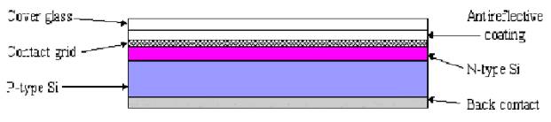
PV’s are
made from semi-conducting material which has been doped with a different atom
or impurity. Within the PV there are two layers, there are know as the p-type
and the n-type layer or the positive and negative layer. The materials used in
the manufacture of silicon have four electrons in the outer electron shell. The
impurity is added to the base material such as silicon which has either one
electron more in the outer shell or one electron less. The commonly used term
for this process is called doping. The result of doping is the creation of
places within the crystalline structure of the base material which have an
excess electrons (n-type) and places where there is a missing electron or a
deficiency (p-type). The missing electron is known as a hole or in other words
a positive charge carrier, while the extra electron acts as a negative charge
carrier. The most common material used in the manufacture of PV is the element
silicon which is one of the most abundant elements on earth. Some of the other
material used in the manufacture of PV are cadmium and gallium. The PV is
composed of the p-type material on one side and the n-type material on the
other side, this creates what is known as a p-n junction. Current flows in the
PV cell when an electron in promoted through the absorption of a photon. The
interaction of photons and the atoms in the PV are essential to the operation
of the PV, with out sunlight then there is not excited electrons and thus no
current. The amount of energy the photon must contain in order to excite an
electron must be greater the band gap energy Eg which is specific to the
material. The energy contained with a photon is a function of the frequency of
light and planks constant h (6.626*x 10-34). This it can be said that the
efficiency of the PV module is dependent on the intensity of light (W/m2)
intercepted by the cell. The stronger the light (the higher the intensity) the
more chance of the absorption of a photon to create an electric current. The
efficiency of the system is governed by the percentage of incoming photons
which cause absorption. Most of the photons absorbed by the cell do not contain
greater than the Eg value required and thus only increase the temperature of
the cell.
BIPV
technology differs somewhat from other application of PV where there are
different criteria. One of the most important considerations of BIPV technology
is its ability to be both a building façade as well as an electricity producing
technology. This can be a used as a very strong economic motivating factor as
the perceived cost of the system is reduced due to the elimination of the need
for other cladding. Design of BIPV really requires an all encompassing approach
towards building design, the various energy systems used within the building
and their interaction together. In this way the maximum benefits of BIPV can be
reaped.
The amount
of electrical power which can be obtained from a BIPV system is directly
related to the availability of solar radiation, this means the orientation, the
tilt and angle and the area of PV façade are of critical importance. The system
should be design so that the demand profile of the building is matched as close
as is possible to the supply profile from the system. This will have direct
effects on the necessity for Balance Of System components such as battery’s and
inverters. The economic viability will be highly dependent of the cost of
electricity from the utility company and the electric loads within the
building.
As with
the other integrated renewable technologies an understanding of the basic
principles of BIPV is essential to produce a BIPV design which does justice to
potential of BIPV at the particular site and building in question.
One of the
key factors which positively influences the case for BIPV in commercial
applications is the ability of the BIPV in some applications to closely match
the supply and demand profiles both daily and throughout the year.
The three
main types of materials used in for PV modules are
- Monocrystalline or
single crystalline silicon
- Polycrystalline or multi
crystalline solution
- Thin film
Mono crystalline silicon is usually produced by the Czochralski technique. This consists
of dipping a monocrystalline seed into molten polycrystalline. Once the seed is
removed a monocrystalline or single-crystalline crystal ingot is formed. The
ingots then go through many processes before finally ending up as a PV cell or
array. The main processes are sawing the ingots, doping, polishing,
interconnecting of the cells and assembly into PV modules and arrays. The
thickness of the wafers used for the manufacture of monocrystalline cells is
about 200 to 400 micrometers. The atomic structure of the monocrystalline is
very much an ordered structure. It is the high degree of atomic order the
allows the efficiency to be as high as 15%. Although real efficiencies will
certainly be lower than this. Monocrystalline cells tend to be reliable when
exposed to potentially harsh environments.
Polycrystalline silicon is manufactured using either the ribbon growth method where
silicon is grown as wafers or sheets which are around the same thickness as
that necessary for PV cell manufacture. Alternatively a block of
polycrystalline silicon is sliced to produce the size of wafer required. Unlike
monocrystalline cells the atomic structure of polycrystalline is not regularly
ordered. Polycrystalline consists of small grains of monocrystalline spread
throughout the polycrystalline. This means that as the flow of current or
electrons is reduced thus the efficiency of polycrystalline is lower than that
of monocrystalline cells. Conversion efficiencies of around 9 to 12% of likely
although real efficiencies are likely to be much less.
Thin film cells are
made by depositing thin semi conducting layer onto a substrate material such as
glass, metal or plastics. The light absorptivity of thin films is much higher
than for crystalline materials, thus the deposited layer can be very thin. The
thickness of the deposited layer is form a few micrometers to as little as one
micrometer. Generally the thinner the
deposited layer the cheaper the manufacturing costs. Spraying is often the
technique used for depositing the thin layer of the semi conducting material.
The manufacturing process for thin films as opposed to monocrystalline or
polycrystalline cells is much faster and uses considerably less energy. Thin
film cells have much lower efficiencies than crystalline materials. This is a
result of the non crystalline structure of the semi conducting layer. Much has
been talked of how thin film technologies can produce low cost environmentally
friendly electricity.
Amorphous silicon (a-Si) is by far the most commonly used thin film material. A-Si has a
disordered atomic structure. The main problem with a-Si apart from the low
efficiencies (real efficiencies of around 4% are likely) is the tendency for
a-Si cells to suffer from degradation on exposure to sun, wind, rain and
atmospheric pollutants. A-Si is likely to lose around 10 to 15% of their
electricity producing capacity within the first few months. A-Si cells tend to
oxidise and are thus much less durable than their crystalline counterparts.
Cadmium
Telluride (CdTe) is a polycrystalline semi conducting compound made from
Cadmium and Tellurium. The absorptivity of CdTe is high, thus CdTe can be as
thin as 1 micrometer and can absorb around 90% if the solar spectrum. CdTe is
also relatively cheap to manufacture. The deposition of CdTe is usually carried
out by spraying, screen painting or high-rate evaporation. A conversion
efficiency of CdTe is likely to be slightly higher than for a-Si. CdTe suffers
from most of the same problems as a-Si such as reliability problems and
degradation or exposure to the environment.